So far, we have used the OpenSDA USB which connects to an ARM debugging chip which is serially connected to the KL46Z256. This can interface with the red LED. We can also interface with a segment LCD, magnetometer, and accelerometer.
The chip has a lot of pins surrounding it, and it is isometric, so we can match the dot on the diagram with a dimple on the chip. Note that some pins are labeled similarly, e.g. PT means port.
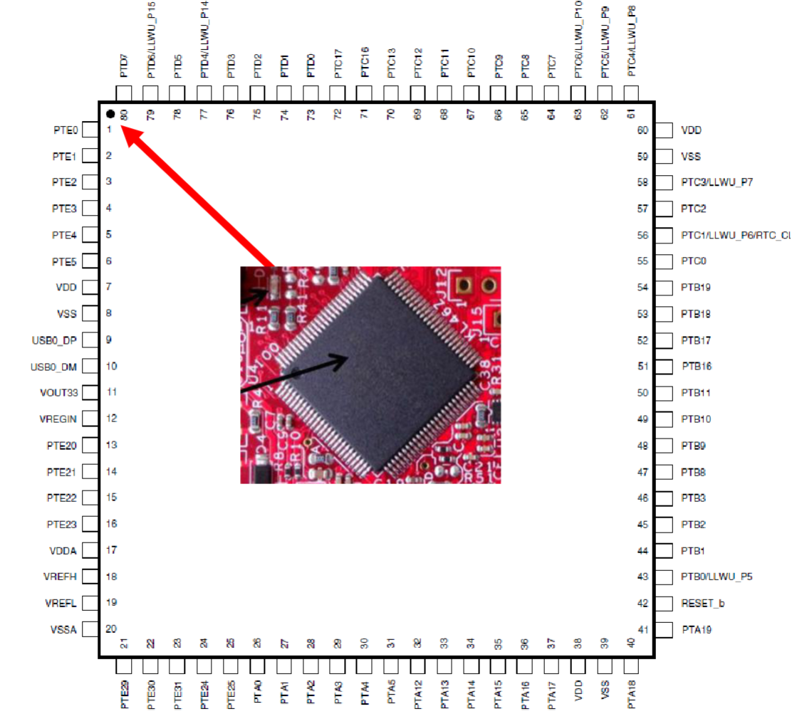
If you wanted to hook up other electronics to the chip, you would hook it up to one of the port pins. It is important to use current-limiting resistors as to not burn out the port.
A general-purpose input and output (GPIO) can be thought of as a switch. It can read whether an input signal is 1 or 0, and it can output 1 or 0. The signal’s value is determined by voltage through the pin as a function of supply voltage ($V_{DD}$). For us, the supply voltage is 3.3 volts.
Since we have a maximum current, we need a resistor with a minimum resistance.
How do we read and write data to and from the GPIO? We could directly connect a register with a pin, or we could add additionally circuitry and muxes.
In the Z80 ISA, there were specific instructions:
out (243), Awould output the value in register A to port 243.in A,254would read the value in port 254 and store it in register A.
The SNAP ISA mapped register 15 to input/output.
For us, we use memory-mapped I/O, so we treat interactions with I/O as if they were memory operations (implemented using muxes). GPIO devices on the chip would go in the peripheral memory space while off-chip (but could be on the same PCB) devices would go in the external device memory space.
Each peripheral slot has a lot of bytes to interact with, so you don’t need to use all of them.
On our chip, we have way more functionality than pins, which explains why we have a mux. If we can multiplex and select whether to connect to pins or one of the many functions, then there is more flexibility.
If you want to use GPIO, you set MUX = 001 by writing 1<<8 = 0x100 to PORTX_PCRn.
There are also data direction registers in the memory. It can be dangerous to drive a line that is connected to something else, so we default to input.
The LED code for lab 1 can be broken into three pieces:
- Turn on the clock.
- Mux to the LED.
- Set direction to output.
There are memory locations called Port Set Output Registers that can set all the bits that are 1 in the register to 1 in a port. It can also clear certain bits and invert certain bits.
In our LEDON and LEDOFF code, LEDON uses PCOR while LEDOFF which is PSOR, which is counterintuitive because we have high voltage turning off the LED and low voltage turning it on. This is because electronics used to be that turning off a current was easier than turning on a current.